NVIDIA GeForce GTX 480 - GF100 Has Landed
 Date: March 29, 2010
We've learned a lot about NVIDIA's GF100 (Fermi) architecture over the past year, and after what seemed like an eternal wait, the company has officially announced the first two cards as part of the series; the GeForce GTX 470 and GTX 480. To start, we're taking a look at the latter, so read on to see if it GF100 was worth the wait.
When NVIDIA first announced its GF100 architecture last fall at the company's own GPU Technology Conference, there was an undeniable focus on having the GPU act as a CPU in many different regards. Given that this conference is more developer-focused, NVIDIA set out to prove the effect that CUDA could have not only in gaming, but in applications as well.
Since that time, the company has seemingly stepped back from pushing CUDA quite so hard, and in the past couple of weeks has shifted its focus back to the pure gaming aspect. During a briefing almost two weeks ago, the company made almost no mention of CUDA or GPGPU, but rather talked mostly about the GTX 480's excellent gaming performance - especially where DirectX 11's tessellation feature is concerned.

The past six months have been rather difficult for both NVIDIA and consumer alike, as both sides have been eagerly awaiting the launch of the company's first GF100-based (Fermi) graphics cards. The long wait is over, though, and AMD's Radeon HD 5000 series finally has some competition. Given the extra time NVIDIA spent on GF100, can we expect that its latest releases can give the HD 5000 series a run for its money?
We took a thorough look at GF100 a couple of months ago, and I recommend reading through that article if you want to see all of what Fermi brings to the table. I won't rehash what was said there, but to put it simply, NVIDIA touts GF100 as being the ultimate gaming architecture, and one that can increase computational performance by as much as 3.5x (this can include CUDA and physics). The company also stresses its dominance where tessellation is concerned, as mentioned above.
As you would expect with a product such as GF100, which is based on a revamped and rethought-out architecture, the improvements NVIDIA brings is going to make its aging GT 200 architecture look out-of-date. We have far better capabilities all-around, and will see nice competition between it and AMD's own offerings.
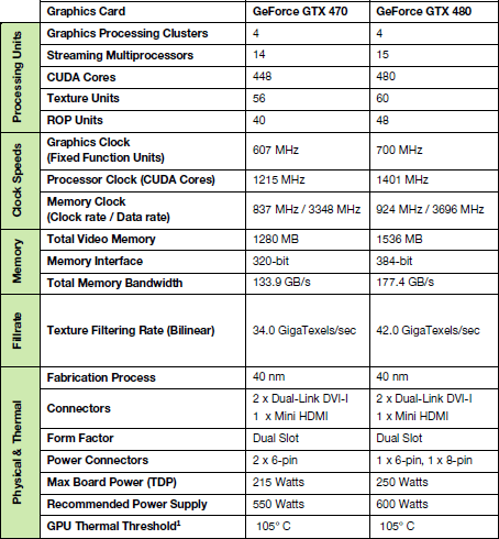
One of the easiest ways to compare one generation to the next is to take a look at all of the company's current models in a table, so we've provided that below. You can see that the GTX 480 (which NVIDIA compares mostly to the GTX 285) has twice the number of CUDA cores, and also features higher clock speeds. It's also had its memory bus decreased from 512-bit to 384-bit, but we've seen the overall density receive a boost from 1GB to 1.5GB.
Model | Core MHz | Shader MHz | Mem MHz | Memory | Bus Width | Processors |
| GeForce GTX 480 | 700 | 1401 | 924 | 1536MB | 384-bit | 480 |
| GeForce GTX 470 | 607 | 1215 | 837 | 1280MB | 320-bit | 448 |
| GeForce GTX 295 | 576 | 1242 | 1000 | 1792MB | 448-bit | 480 |
| GeForce GTX 285 | 648 | 1476 | 1242 | 1GB | 512-bit | 240 |
| GeForce GTX 275 | 633 | 1404 | 1134 | 896MB | 448-bit | 240 |
| GeForce GTX 260 | 576 | 1242 | 999 | 896MB | 448-bit | 216 |
| GeForce GTS 250 | 738 | 1836 | 1100 | 1GB | 256-bit | 128 |
| GeForce GT 240 | 550 | 1340 | 1700 | 512MB - 1GB | 128-bit | 96 |
| GeForce GT 220 | 625 | 1360 | 790 | 1GB | 128-bit | 48 |
| GeForce 210 | 589 | 1402 | 790 | 512MB | 64-bit | 16 |

As the process shrinks, so does the physical size of the die. Well, as long as the transistor count doesn't drastically increase during the next-generation, which isn't the case here. In fact, I almost wonder if GF100 sets a record, with its 3.2 billion (!) transistors resulting in a die-size of 529mm2. Compare that to the 2.15 billion (334mm2) for AMD's Radeon HD 5870 or to the 1.17 billion (258mm2) for Intel's six-core Core i7-980X Extreme Edition!
Unfortunately, the screws on the back of my particular sample refused to cooperate, so to avoid stripping them, I am falling back on this make-shift graphic above to show the size difference between the HD 5870 die and the die on the GTX 480. As you can see, one is certainly larger than the other... 58% larger in volume, to be precise.
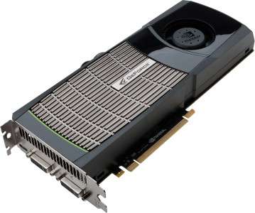
Before we get into performance testing, let's first take a deeper look at the card itself, including its design and features.
Link Here: www.sti.edu

1 comments:
san b mabili yn mga yn??^^
Post a Comment